I’m not ready to give up on these speakers just yet. They sound great, but the control LCD is messed up. I wonder if I can get it working even better than before. I ended up reverse engineering some mysterious components, and hopefully my experience can teach you a thing or two about the process.
Update: Part 2 is now available.
- The story
- The problem
- First guesses
- Technique
- Results
- Take a step back
- Replacement plan
- Arduino
- Next steps & code
- Who’s Varun?
The story

After my first summer internship, I bought my first (and only) set of speakers: Logitech’s Z-680. It’s a 5.1 speaker set with three main inputs (coax, optical, analog), and an aux input which mixes into whatever else is playing. It is supposedly THX-certified and rated up to 505W output. I usually run it at the lowest volume/subwoofer settings, and the audio quality is excellent.
The system is designed in a pretty cool way. The amplifier is in the same cabinet as the subwoofer, and the other speakers connect to the subwoofer. The freestanding “control pod” has inputs, buttons, IR receiver, and status LCD. It connects to the amp/sub through a screw-in D-Sub connector.
The problem
After 13 years, the speakers sound great, but there were some minor and major issues. The remote control stopped working, but that just needed to have its carbon pads cleaned up a little.
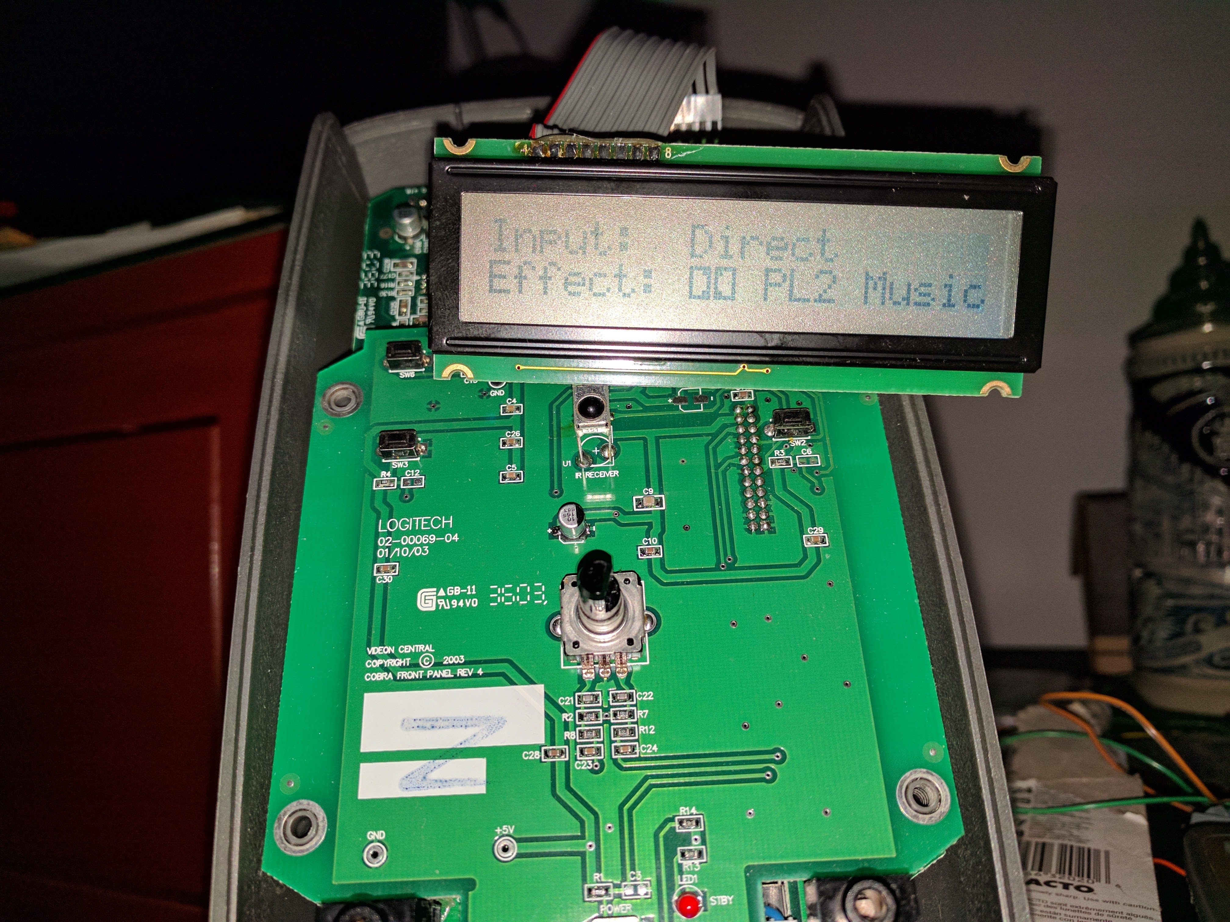
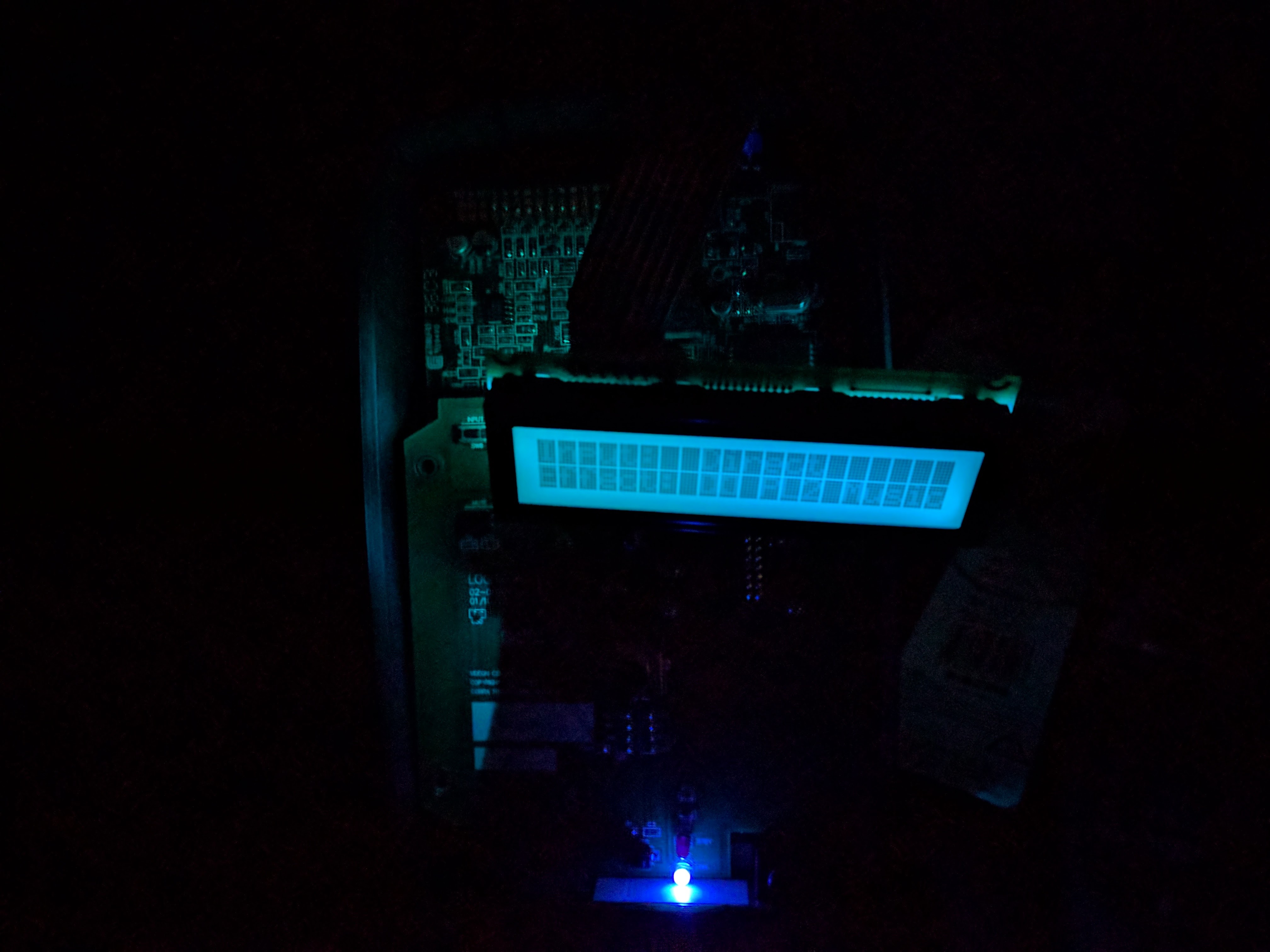

The major issue is the LCD on the control pod. There is no contrast adjustment, and the LCD has been fading with age. The blue backlight looked cool when it was new, but it has dimmed and started to flicker. This leads to some particularly ugly results, and makes it much harder to use the speakers. These photos underrepresent the severity of this problem.


I took the control pod apart, and I learned:
- The LCD is a completely separate module from the other boards!
- The LCD is a 2x20 character LCD. That is, 2 rows of 20 characters each.
- There’s no contrast adjustment.
- Just 8 wires connect the LCD to the main board.
Fixing the existing display appears to be impossible, but can I replace it? The first step in replacing it will be to understand how the LCD communicates. If I can learn more about it, I might be able to find a direct replacement. The LCD module is labeled as being manufactured by VDS. Some quick searches reveal that several other people have run into the same problem, and have had no luck in finding a replacement. In fact, the manufacturer, VDS, has since gone out of business. I’m going to have to reverse engineer the LCD protocol in order to make any progress.
First guesses
This LCD is clearly a character LCD, used specifically for the display of textual information rather than graphics. A very common protocol used for character LCDs is the 4/8-bit parallel one used in the Hitachi HD44780 controller chip from 1987. That design has been copied by pretty much everyone else making similar displays. I would guess that this LCD is also using that protocol. If so, all I have to do is identify which pins are being used for which purpose. Since we only have 8 pins, I would expect:
- Vcc pin, probably 5V
- GND pin
- LATCH pin
- Command/Data pin
- 4 parallel data bit pins
Technique
Safety
Before hooking any of my equipment up to the pins, I need to check voltages and make sure everything is safe. I’ll also be able to put in an initial guess on pins and their functions. Luckily, the main board has a test point labeled ‘GND’ which I can use as a reference. Checking with a voltmeter, in different states, I get the following voltages:
| Pin | STDBY | ON |
|---|---|---|
| 1 | 5 | 5 |
| 2 | 0 | 0 |
| 3 | .13 | .13 |
| 4 | 5 | 5 |
| 5 | 0 | 5 |
| 6 | 5 | 5 |
| 7 | .12 | .12 |
| 8 | .12 | 4.5 |
Nothing went above 5V no matter what I did. It’s not a guarantee, but I feel safe enough connecting my equipment to check things further. Pins 1 & 2 are likely Vcc and ground, which means we’re probably working off of 5V logic. Pins 7 & 8 are not tied to the same ground reference, which means they might be for a separate function; they are probably for the LCD backlight, which only turns on in the ‘ON’ state. That leaves only 4 pins for logic, 3-6, which we’ll have to investigate.
Logic analysis
The same logic analyzer that help me with getting an i2c sensor working is back in action. I set my DSLogic to 5V logic, and attached probes to all 8 LCD pins on the main board. I captured the traces, and I found only pins 4, 5, and 6 had anything interesting happening. It was not at all what I was expecting.

This is not parallel. This is serial. Specifically, this looks exactly like a Serial Peripheral Interface (SPI) connection, which alongside I2C, I2S, and UART, shows up in many embedded devices.
Results
Protocol decoding
I used my logic analysis software’s protocol decoder, and I captured the data on these three pins. Pin 4 appears to be Chip Select (CS), Pin 5 is Master Out Slave In (MOSI) data, and Pin 6 is the Clock (CLK). CS goes high every three bytes, which implies that every instruction to the LCD is three bytes long. I found these patterns were sent at power-up, and decoded them with the default SPI settings. Here’s some of that data.
F8 00 10  FA 00 80  FA 00 80  FA 00 80  FA 00 80  FA 00 80  FA 00 00  FA F0 80  FA 00 00
FA 20 00  FA 20 00  FA 20 00  FA 20 00  FA 20 00  FA 20 00  FA 00 00  FA F0 80  FA 00 00
This continues with more data of the form FA X0 X0 and a few like F8 X0 X0. A total of 300 bytes are sent at startup, and then whenever the unit is turned on and any buttons are pressed. I had to figure out what these sequences mean. Even if it isn’t an HD44780-like parallel interface, it likely still sends some commands and even more data. I figure F8 comes before a command, and FA comes before the data. That means the remaining 2 bytes are the payload for the LCD controller.
Data decoding
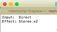
What the heck do all these bytes mean? There has to be some logic to which byte payloads mean what. I hoped that each letter mapped to a consistent payload; if it did, then I could start decoding the LCD’s messages. To pull it off, I would need to match some byte streams to some known text. When switching inputs, you get messages like
Input:  Optical
Effect: Detecting...
along with a stream of bytes flowing across the data line. You get some F8 sequences, and exactly 40 FA sequences. This LCD can only display 40 characters. This confirms to me that FA is used for data bytes, specifically for each letter. Line up the FA payloads with each character, and you get:
| I | n | p | u | t | : | O | p | t | i | c | a | l | |||||||
|---|---|---|---|---|---|---|---|---|---|---|---|---|---|---|---|---|---|---|---|
| 90 20 | 70 60 | 00 E0 | A0 E0 | 20 E0 | 50 C0 | 00 40 | 00 40 | F0 20 | 00 E0 | 20 E0 | 90 60 | C0 60 | 80 60 | 30 60 | 00 40 | 00 40 | 00 40 | 00 40 | 00 40 |
| E | f | f | e | c | t | : | D | e | t | e | c | t | i | n | g | . | . | . | |
|---|---|---|---|---|---|---|---|---|---|---|---|---|---|---|---|---|---|---|---|
| A0 20 | 60 60 | 60 60 | A0 60 | C0 60 | 20 E0 | 50 C0 | 00 40 | 20 20 | A0 60 | 20 E0 | A0 60 | C0 60 | 20 E0 | 90 60 | 70 60 | E0 60 | 70 40 | 70 40 | 70 40 |
We’re on to something; we’ve found some consistency. Each time we see the letter i, for example, we get 90 60. But this still doesn’t make sense. I would think that D and E would have adjacent hexadecimal values, but they are 20 20 and A0 20, respectively. We could throw away the second half of each byte, since that’s always 0, but that still gives us 22 and A2. What are we doing wrong?
Take a step back
I’ve been interpreting all the data from the logic analyzer as hexadecimal values, but what if we’re looking at it the wrong way? I break down some of the letters into hex and binary, so we are looking directly at the raw MOSI and CLK pulses. We’ll still throw away the half-bytes that are always 0
| Letter | Code (hex) | Code (binary) |
|---|---|---|
| D | 20 20 |
0010 0010 |
| E | A0 20 |
1010 0010 |
| I | 90 20 |
1001 0010 |
| N | 70 20 |
0111 0010 |
| O | F0 20 |
1111 0010 |
| a | 80 60 |
1000 0110 |
| c | C0 60 |
1100 0110 |
| e | A0 60 |
1010 0110 |
| f | 60 60 |
0110 0110 |
| g | E0 60 |
1110 0110 |
| i | 90 60 |
1001 0110 |
| l | 30 60 |
0011 0110 |
| n | 70 60 |
0111 0110 |
| p | 00 E0 |
0000 1110 |
| t | 20 E0 |
0010 1110 |
| sp | 00 40 |
0000 0100 |
| : | 50 C0 |
0101 1100 |
Okay, I think we have figured this out. Look at D and E in binary, and you see that we just added 1 in the most significant bit. You see the same between f and g. Now look at e and f: we literally add 1 and had the carry move down to the next bit. We are reading the bits in reverse order. The Z680 control pod uses Least Significant Bit (LSB) instead of Most Significant Bit (MSB) first.
When we decode everything properly, D is 44 and E is 45. It’s all ASCII! Now we know how to decode the characters, but we can also look at the commands. We can now retranslate some of the commands we saw, and try matching them up to HD44780 codes. We get:
| Wrong | Right | “Actual” | HD44780 Meaning |
|---|---|---|---|
F8 00 30 |
1F 08 00 |
CMD: 08 |
Move cursor to position 0 on display. |
F8 40 00 |
1F 02 00 |
CMD: 02 |
Reset cursor to home. |
F8 20 90 |
1F 04 09 |
CMD: 94 |
Move cursor to position 20 on display. (start of line 2) |
Yup, this is just a funny serialized version of the HD44780 parallel protocol. Specific notes on the protocol implementation:
1Fis used for commands, and5Fis used for data.- The high nybbles of both payload bytes are thrown out.
- The low nybbles are used.
- The first low nybble is the low nybble of the “Actual” data.
- The second low nybble is the high nybble of the “Actual” data.
-
Command
08is supposed to move the cursor to position 0 of DDRAM, but it actually moves to position 0 of CGRAM.
Replacement plan
We know pretty much everything about how this LCD and control pod communicate. After searching around, I could not find any serial character LCDs which use the same protocol, which means a simple replacement is impossible.
I’m still going to replace it, but with a parallel character LCD. I’ll need to make a very lightweight converter to unshift the serial commands. It will have to know how to handle 1F and 5F byte sequences. It will also have to handle the 08 commands properly, so the control pod can create its custom characters in CGRAM. Might as well do this with an Arduino!
Arduino
A few years back I picked up a bunch of RBBB Arduinos. They’re great as cheap, fully-featured, and tiny Arduino-compatible systems. They do not have a USB UART on-board, to save money, but a single USB BUB adapter can be used for both programming and Arduino <-> PC serial communication.

The RBBB can be cut down a lot, so it should be small enough to fit inside the control pod, along with a replacement LCD module. The broken LCD is very thick, so hopefully we’ll figure out a better way of using the available space. I set it up as follows:
- Control Pod Pin 1 (Vcc) to RBBB 5V Input
- Control Pod Pin 2 (GND) to RBBB GND
- Control Pod Pin 4 (CS) to RBBB Slave Select (SS)
- Control Pod Pin 5 (MOSI) to RBBB MOSI
- Control Pod Pin 6 (CLK) to RBBB SCLK
I have the Arduino converting the hd44780 cursor movement codes into ANSI terminal codes. This can work very well, but it means that we can’t use the standard Arduino serial console. Instead we have to connect with a terminal program, using a command like screen /dev/cu.arduinoserial 115200.

It was a little difficult to find an Arduino SPI slave example, as it is not part of the default Serial library for the platform. When I manipulate the knobs and buttons on the control pod, it’s fun to see the information being updated on my computer.
Next steps & code
Code for this project is available as a GitHub repository. I’ll add a README shortly.
This has been a blast to reverse engineer; we have figured everything out about this LCD system, and we can replace it with whatever we want.
The plan is to get the Arduino working reliably with a parallel character LCD, then somehow fit it all inside the control pod. I’m looking at 2x20 displays to find one that will fit and work well. I think I’ll try and find an OLED; I’m tired of backlights, and OLED feels more like the VFDs of old.
Who’s Varun?
I most recently was the founder of an HR tech startup, Disqovery. I have worn many hats, and I like making things. I also like talking business. You can reach me at me@varunmehta.com, Mastodon, Github, and LinkedIn.